10-Band Audio Equalizer with Dual VU Meters
July 2026
An analog equalizer with ten active band-pass filters, independent input and output gain controls, bypass feature, and dual LED VU meters.
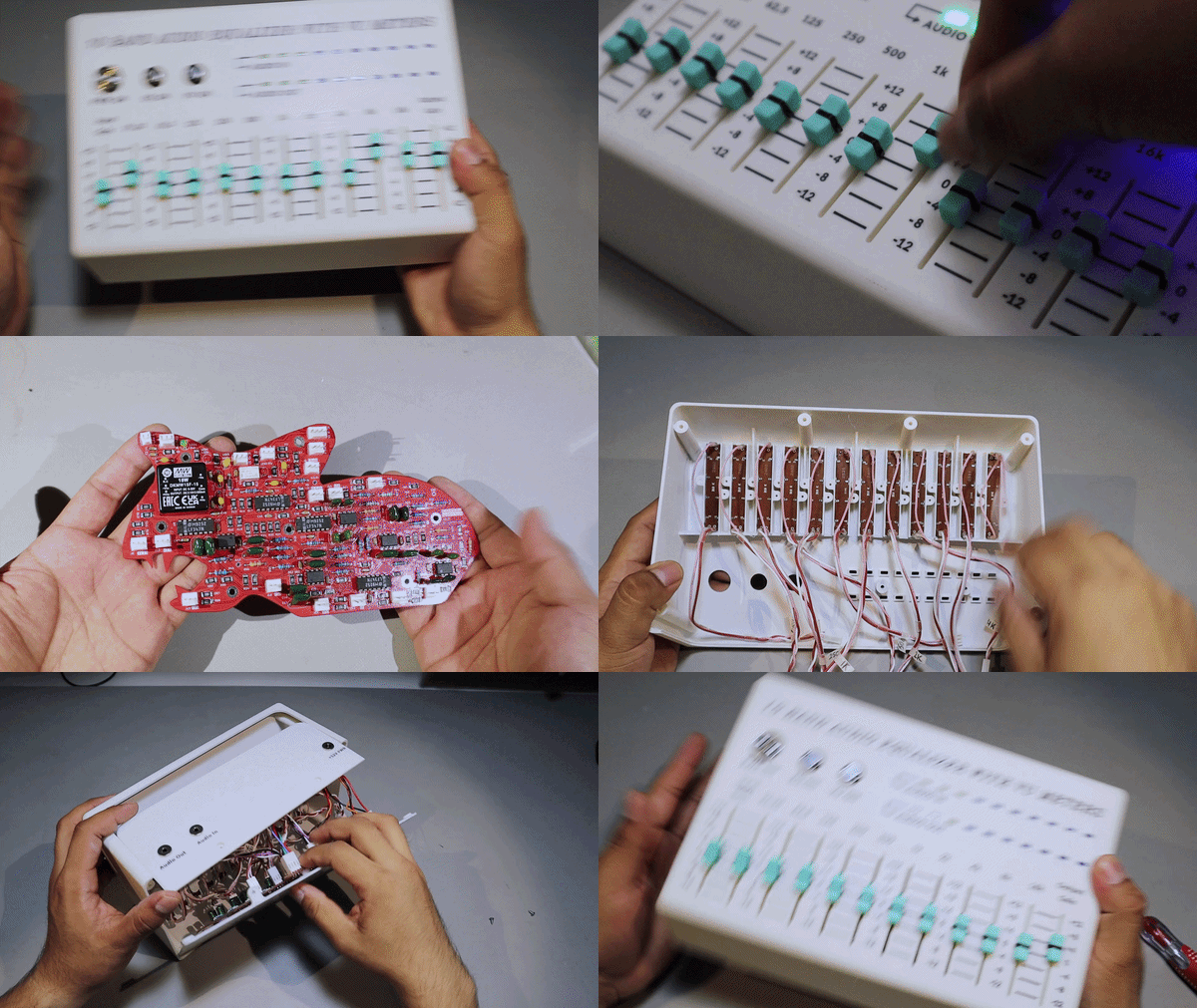
Overview
This project is a fully analog 10-band audio equalizer, a device that allows specific audio frequency ranges to be boosted or attenuated to shape the sound of an audio signal.
Ten band-pass filters provide independent ±12 dB band controls, while separate input and output gain stages provide additional signal-level adjustment. A DPDT relay allows the equalizer to be bypassed for direct comparison between the original and equalized signals. Two 10-segment LED VU meters monitor the input and post-EQ output levels and can be switched off independently.
The following video demonstrates the completed audio equalizer and SolidWorks animation:
A custom 3D-printed enclosure houses the electronics, controls, connectors, and LED VU Meters.
The project combines analog circuit design, LTspice simulation, PCB design, hardware testing, CAD modeling, and 3D printing.
System Overview
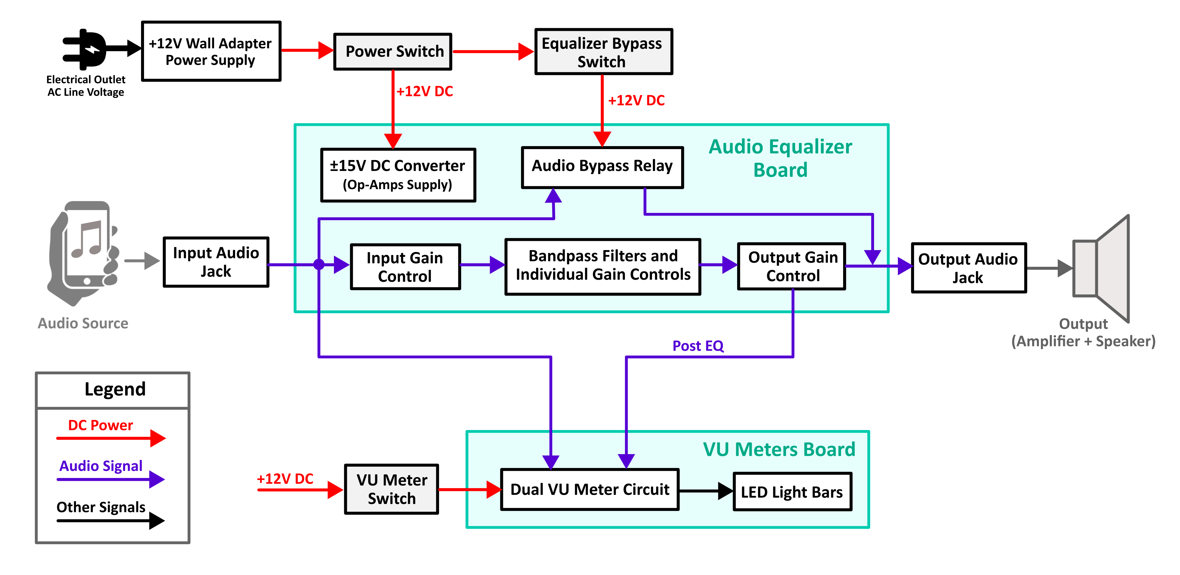
The high-level design for this device is shown in the block diagram below. The system consists of the audio equalizer board, the VU Meters board, the audio connectors and switches.
The figure below describes the audio signal path through the main analog filter circuit. The audio input signal first passes through an op-amp gain stage that allows the input signal level to be adjusted while also providing a high-impedance buffer for the audio source.
The buffered signal is then distributed across ten band-pass filters. Each filter output passes through an independently adjustable gain stage before all ten bands are recombined by a unity-gain summing amplifier.
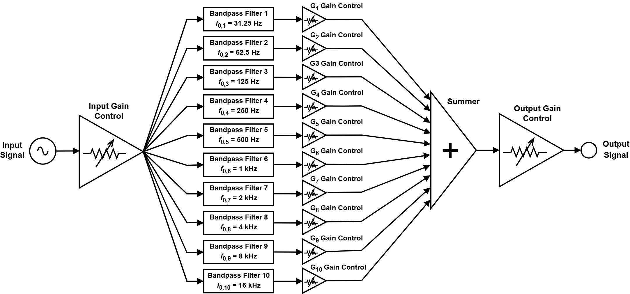
The summed signal then passes through a final op-amp stage that provides overall output gain control. The output can then be connected to an external audio amplifier and speakers.
A DPDT (double-pole, double-throw) relay allows the equalizer to be bypassed from the front panel, making it easy to compare the original input signal with the equalized output.
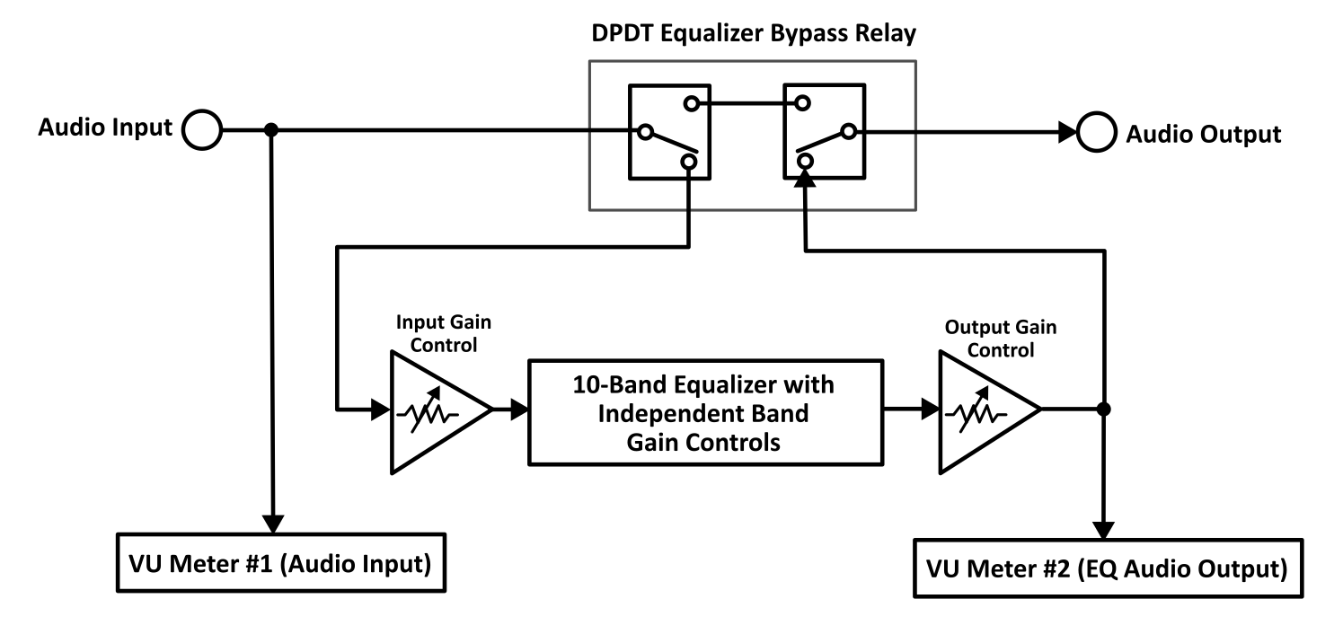
The same system also connects to a dual VU-meter board, which monitors the raw audio input and the post-EQ output signal. The VU-meter board can be switched off independently from the front panel.
Filter Design and Circuit Simulation
The ten band-pass filters were designed using the multiple feedback (MFB) topology, which was selected for its low component count and moderate sensitivity to component tolerances.
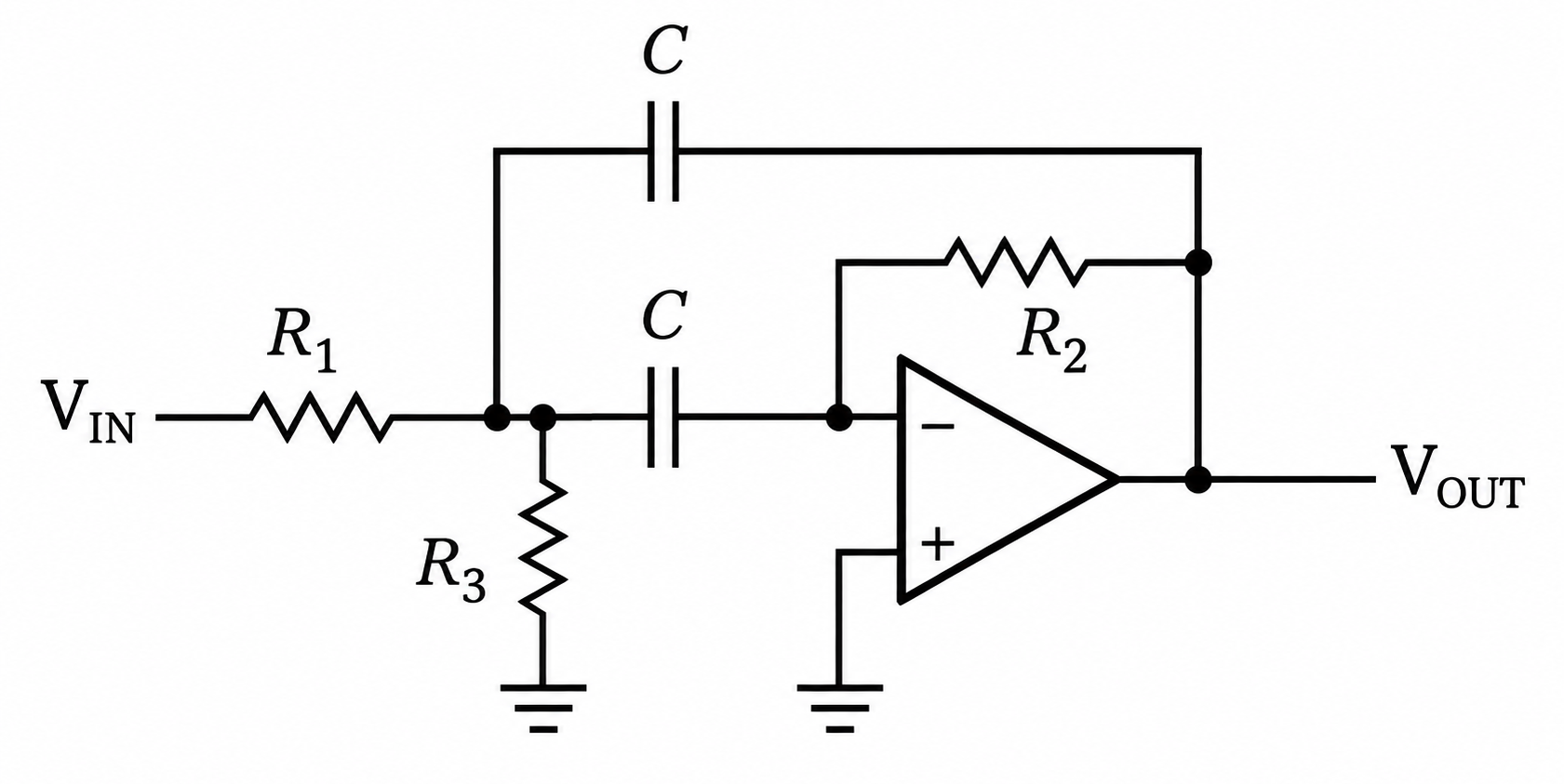
The filters use octave-spaced center frequencies ranging from 31.25 Hz to 16 kHz. Together, the filter bank covers approximately the 20 Hz to 20 kHz audio range.
A quality factor of approximately Q = 1.414 was selected to provide moderate selectivity while allowing adjacent octave-spaced bands to intersect near their -3 dB frequencies. Each band includes an independently adjustable ±12 dB gain stage. Separate input and output gain-control stages provide additional signal-level adjustment before and after the filter bank.
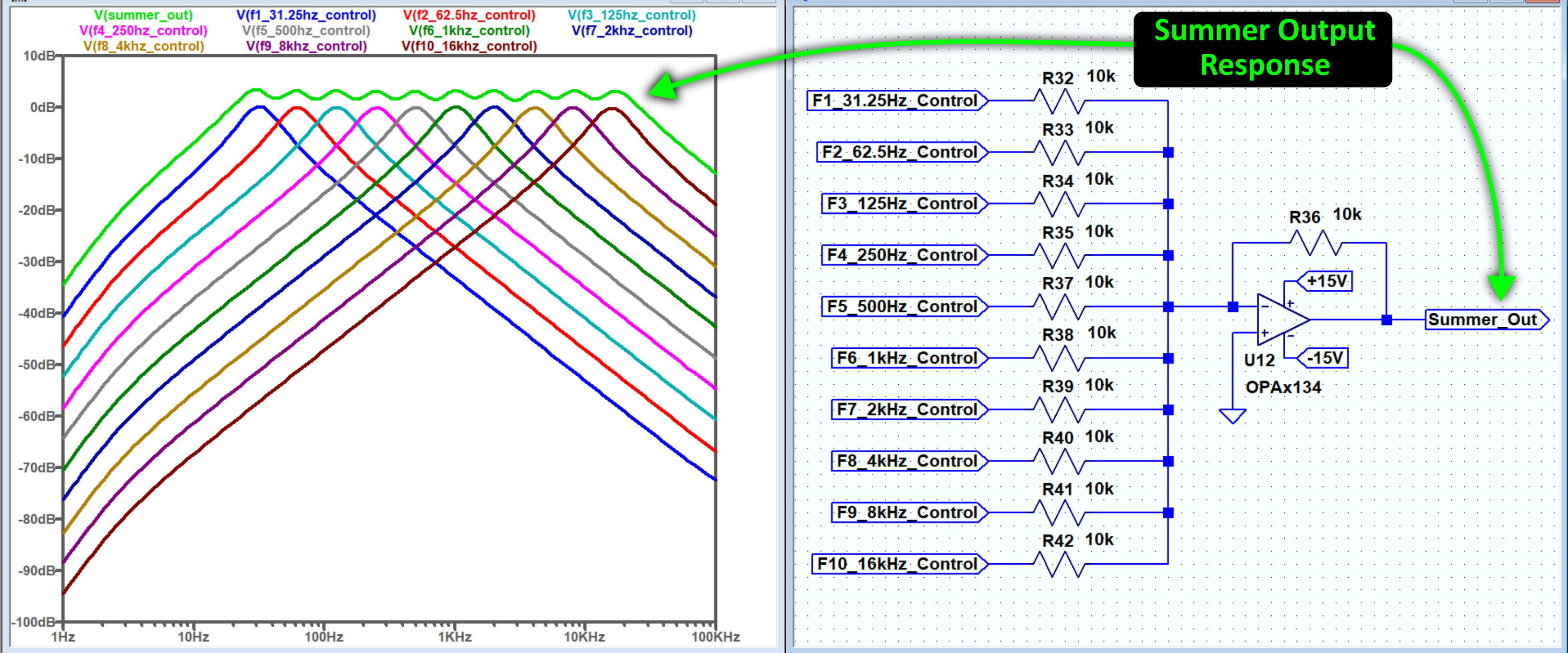
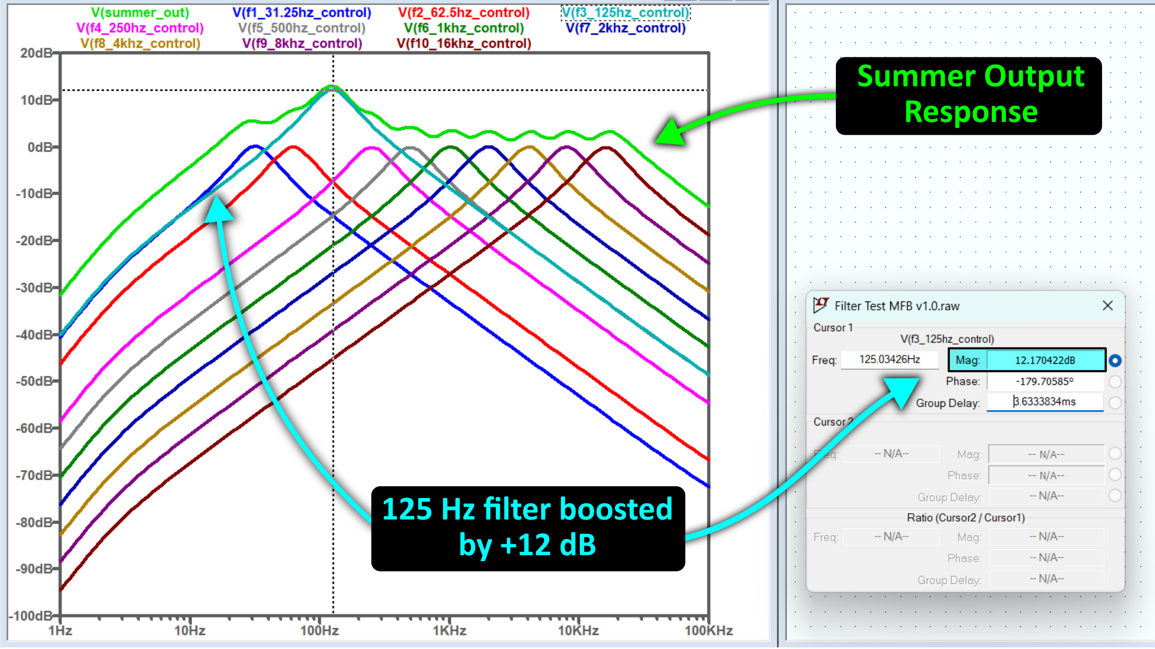
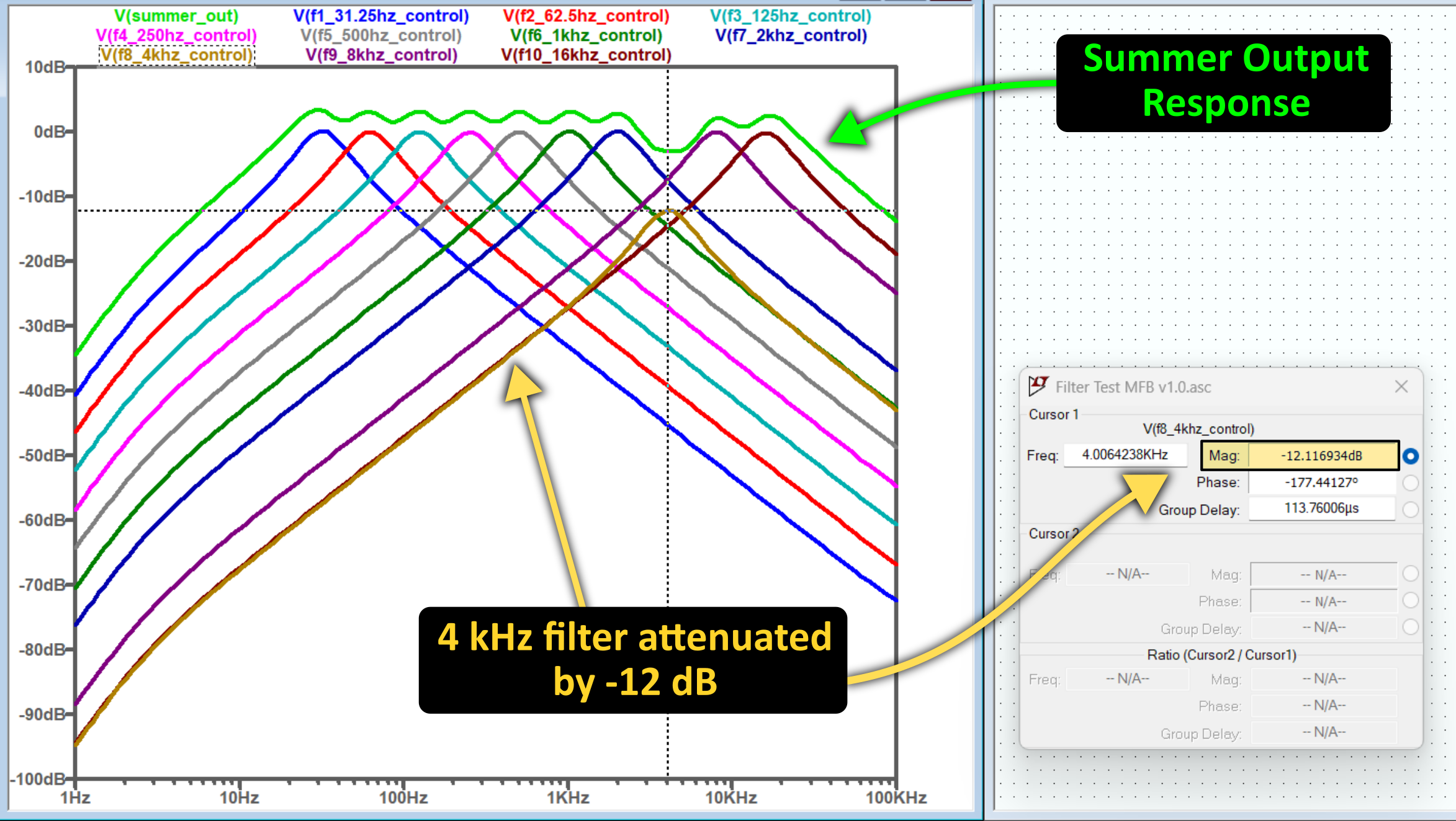
The complete circuit was simulated in LTspice, the Bode plots were used to verify the center frequency and frequency response of each band before the circuit was physically built as shown in the images above.
The Dual VU Meter
The VU-meter circuit was implemented on a separate PCB using two LM3916 LED display drivers. One channel monitors the raw audio input while the second monitors the post-EQ output.
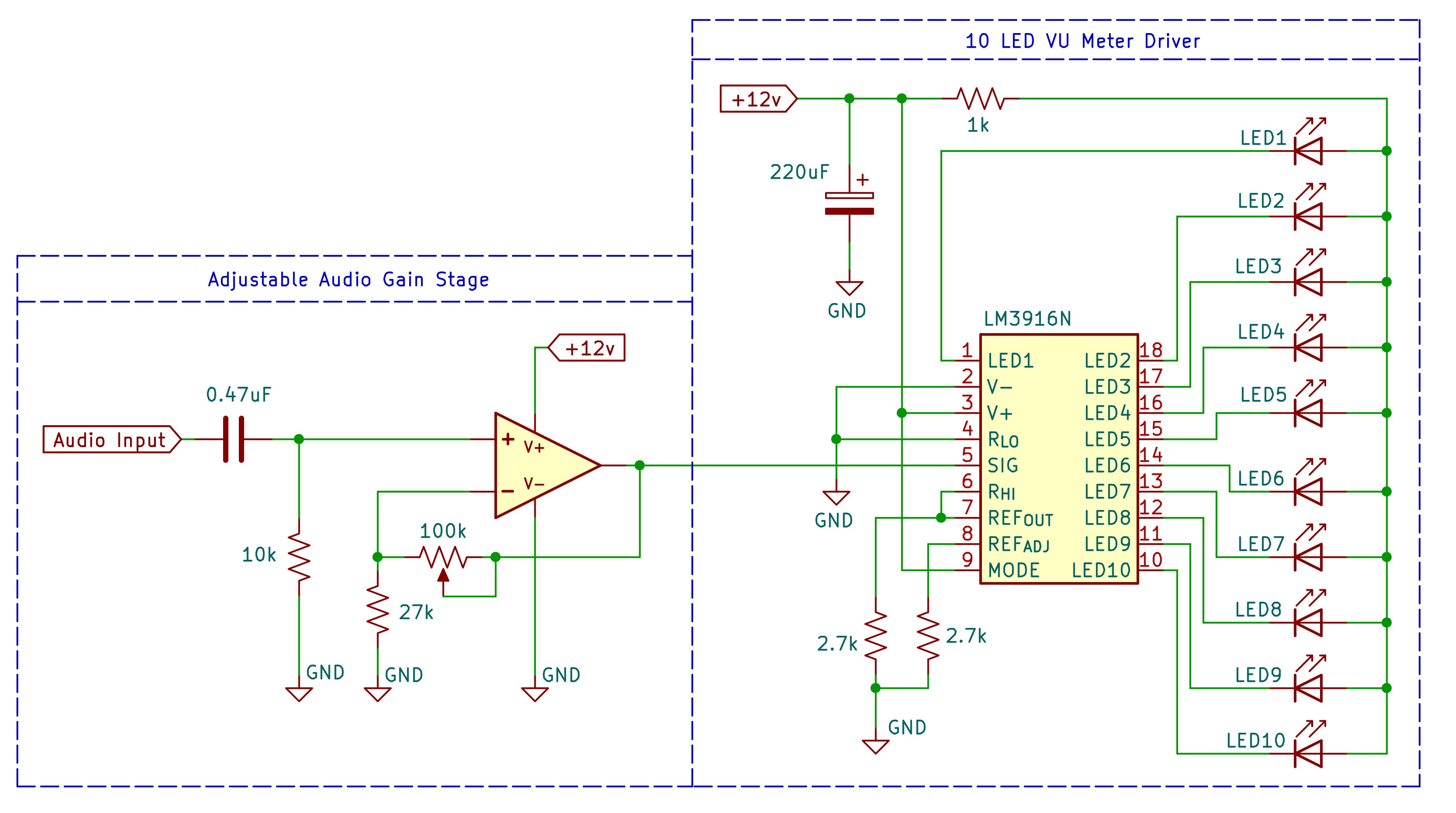
As shown in the schematic above, each channel includes an op-amp input stage that buffers the monitored signal and allows the sensitivity of the VU meter to be adjusted independently. The VU meter board can also be switched off independently without affecting the operation of the audio equalizer.
PCB Design
The PCBs for both the audio equalizer and VU meters were designed in KiCad. The main equalizer PCB contains more than 150 components and uses several Molex KK 254 connectors for power, external controls, and the slide potentiometers mounted on the enclosure.
Loading 3D model…
Drag to rotate • Scroll or pinch to zoom
If you're curious, the PCB shape is supposed to resemble a wildcat (my alma mater's mascot). Unfortunately, my drawing skills (yes, I had to draw this by hand) are laughable to say the least, but hey, it works :D
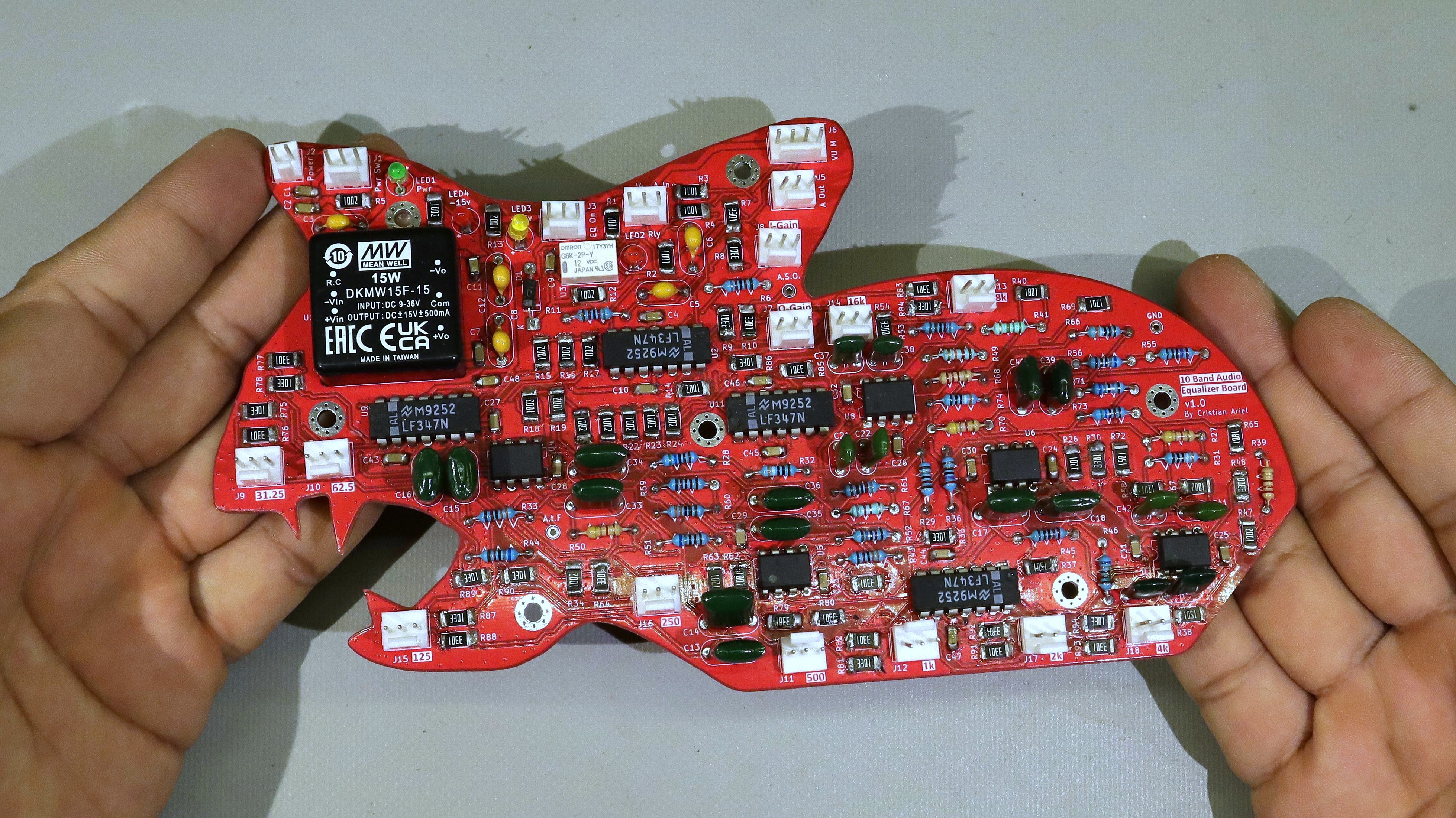
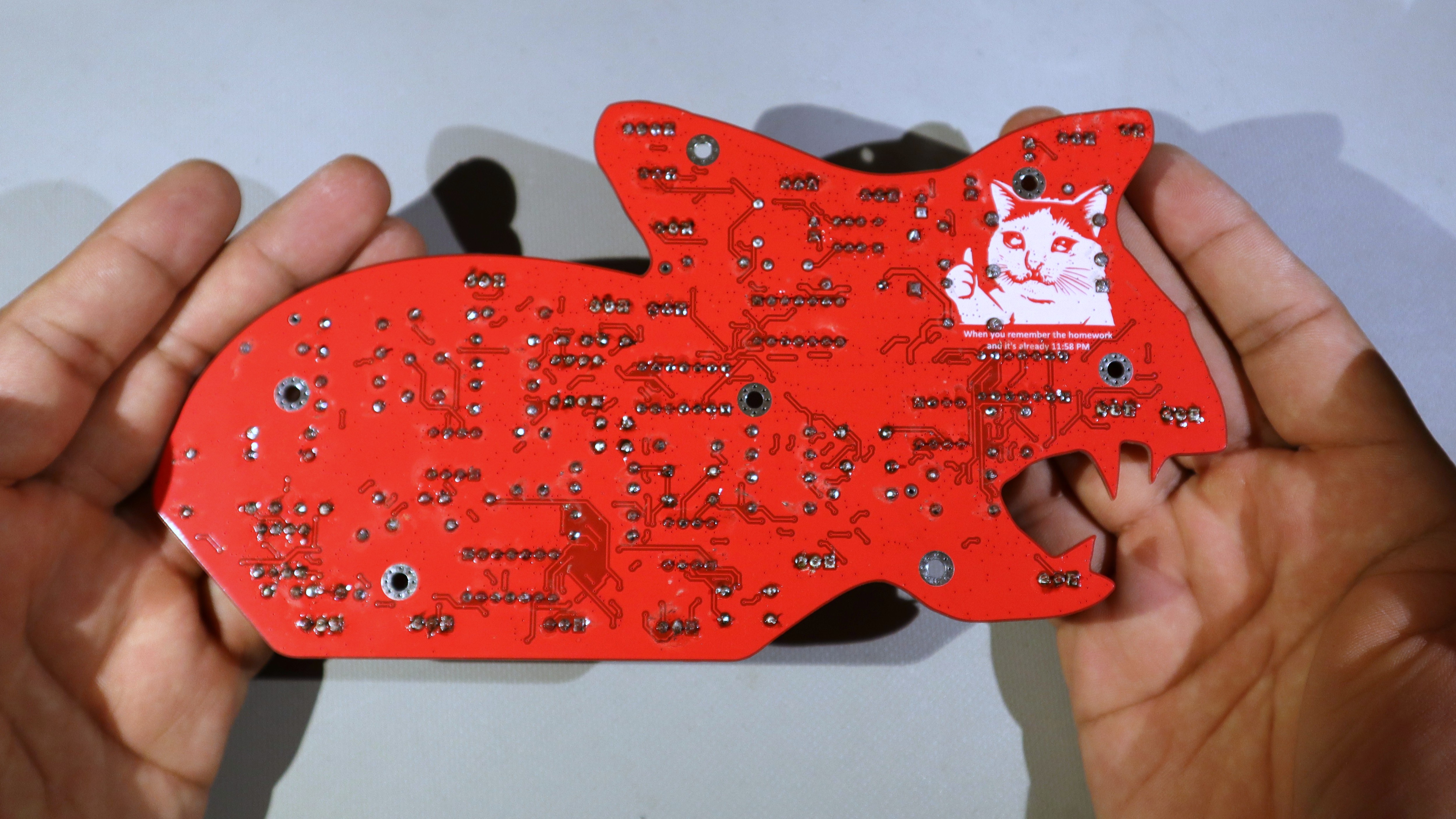
The VU-meter PCB was designed as a separate module so that the LEDs could be positioned directly behind the front panel. This also keeps the design modular, since the audio equalizer can operate without the VU meter board installed.
Loading 3D model…
Drag to rotate • Scroll or pinch to zoom
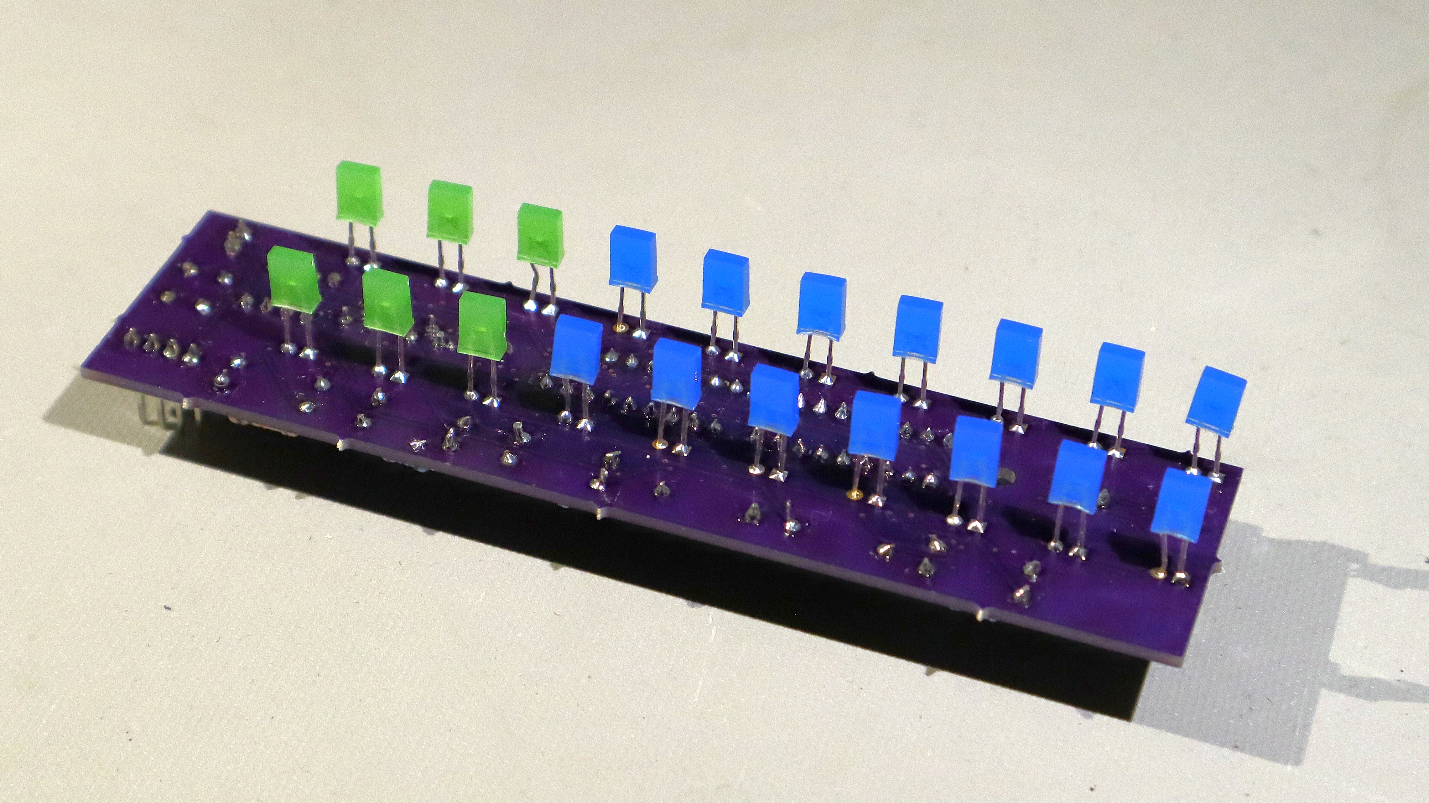
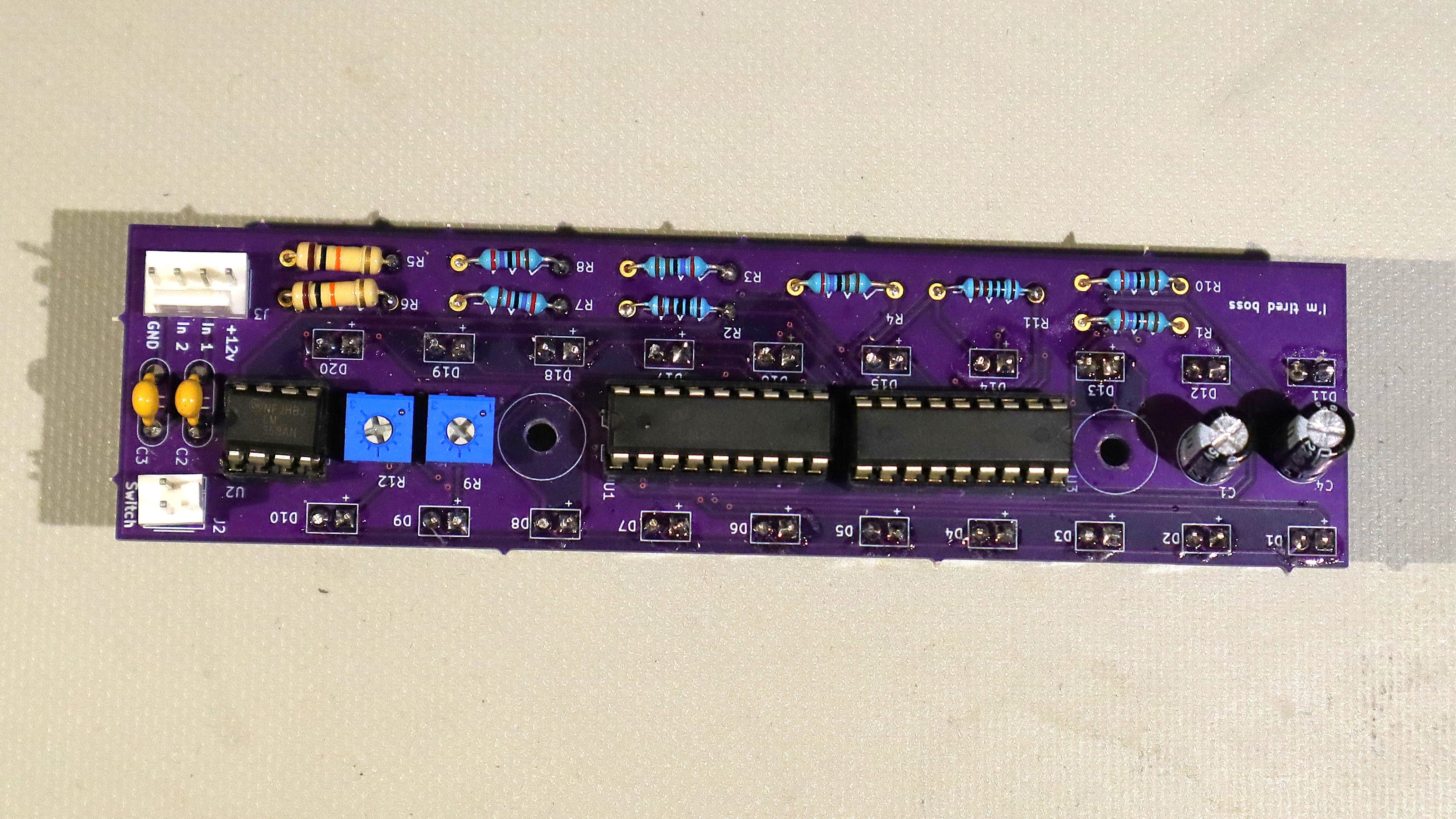
As seen in the image below, each row of ten LEDs corresponds to one VU meter channel. Before installation, the sensitivity of each VU-meter channel was adjusted using the onboard trimmer potentiometers (the blue components shown in the image) to calibrate the meters for their respective signal levels.
3D Design and Assembly
A custom three-piece enclosure was designed in SolidWorks to house and protect the circuit boards, switches, audio connectors, LED displays, and slide potentiometers. Custom slider knobs were also designed for the potentiometers. The enclosure went through several design iterations to verify component fit, alignment, accessibility, and ease of assembly.
Loading 3D model…
Drag to rotate • Scroll or pinch to zoom
All enclosure components were 3D printed and assembled with the completed electronics. For a rendered view of the complete CAD assembly, watch the assembly animation here.
Results
The completed equalizer successfully provided independent adjustment of all ten frequency bands, along with separate input and output gain control. Measured filter responses closely matched the LTspice simulations, with most center frequencies within approximately 1% of their intended design values.
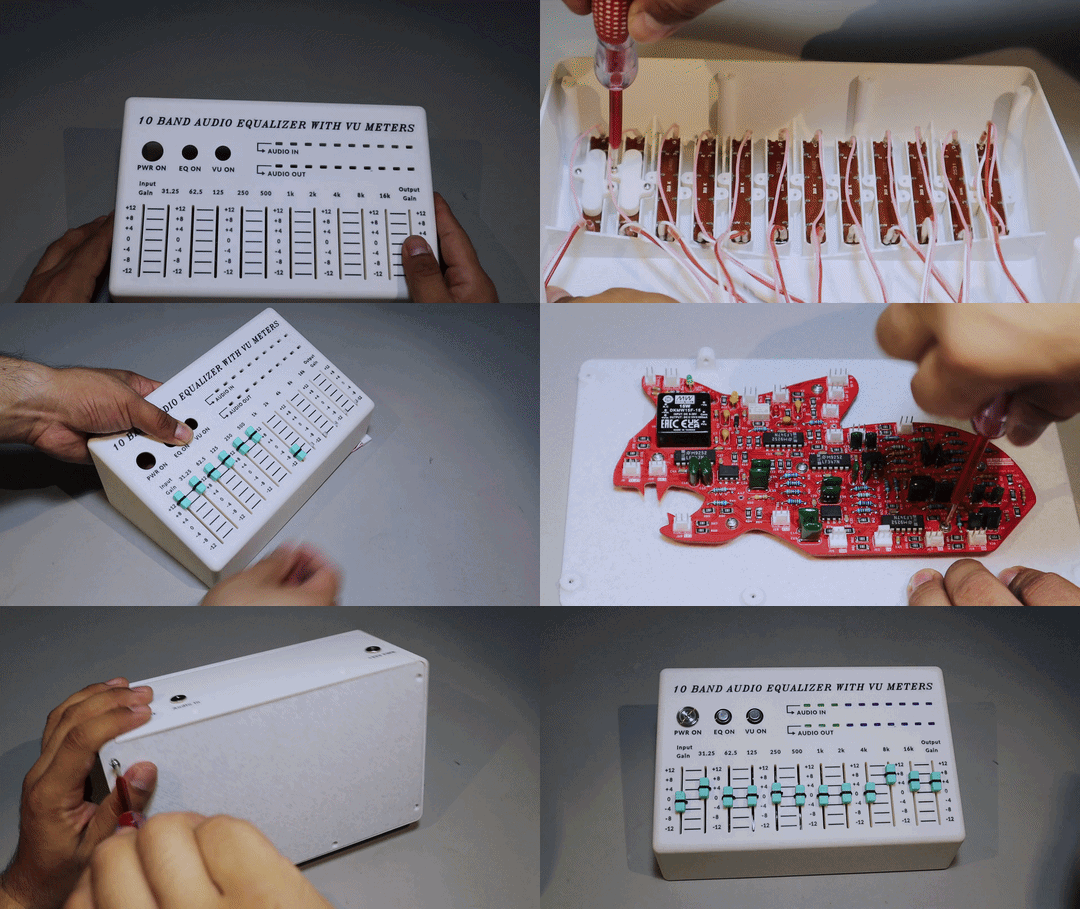
The DPDT bypass relay allowed direct comparison between the original and equalized signals, while the dual VU meters provided visual indication of the input and post-EQ signal levels. The custom 3D-printed enclosure successfully integrated the electronics, controls, connectors, and LED displays into a compact and easy to use final assembly.